This tutorial is about ADC in AVR ATmega32A Microcontroller. ADC stands for analog to digital converter which allows us to interact with physical world. Almost all microcontrollers come’s with built-in circuitry of ADC. ADC allows us to read data from sensor using microcontroller. This way we could able to control, sense and communicate with real world data. Let’s get into little more technical. ADC in AVR ATmega32A Microcontroller is multiplexed with PORTA that means ADC channel are shared with PORTA. The ADC can be operated in single conversion mode and free running mode. In single conversion mode the ADC does the conversion and then stop. While in free running, it used to convert continuously. It does a conversion and start next conversion immediately after that.
How ADC Works?
In real world example, every sensor senses physical parameters (voltage, temperature or pressure etc.) and converts it into equivalent analog signal. But for efficient and ease of signal processing, this analog signal is converted into a equivalent digital value using analog to digital converter. This digital value is then fed into microcontrollers ADC featured pin.
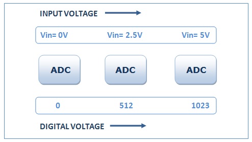
The ADC of AVR has 8 channel and 10-bit resolution
8-channel: This means there are 8 ADC pins are multiplexed together. We can see those pins named as PA0, PA1…..PA7. 10-bit Resolution: This means there are 2^10=1024 steps/counts.
Suppose we use 5V reference. In this case any analog value in between 0V and 5V is converted into its equivalent ADC value. The 0-5V range is divided into 2^10=1024 steps. Using the default reference voltage of 5v and this voltage is converted to a 10 bits value, the resolution of each bit is 5v/1023 = 4.88mV for each consecutive value, but imagine that you have an analog accelerometer, those are almost always 3.3v part, so if you used the 5v reference you would have 5 – 3.3 = 1.7v of unused values and also a reduced resolution, now let’s see what is the resolution if you used an 3.3v reference voltage 3.3/1023 = 3.22mV for each consecutive value, so it’s a gain in resolution and you would be able to use the full range of the ADC.
The internal ADC can also be used in an 8-bit mode, where only the most significant 8 bits of the full 10 bits resolution are used, this might be useful when working in noisy environments and you only need 8 bits resolution, using this mode is a plus because you don’t need to spend extra time shifting the full 10 bits result into an 8 bits.
Let me introduce you something which is important to know that. As our chip is being feed with 5v we can plug any signal that we want to the ADC input pins if the signal is inside the 0-5v range, above or below that and the ADC circuitry will be damaged forever and you might even destroy the whole chip. We can also change(given that its always below the Vcc of chip) the maximum voltage that the ADC uses, for that you can put your desired max voltage(it’s called the reference voltage and it’s against this voltage that all analog to digital conversions are done) in the Aref pin, that is pin 32 of the DIP package and then configure the ADC in software to use that voltage reference, I will not explain this in this tutorial, but if you have doubts just shoot a question.
Let’s understand ADC Prescaler and ADC Register:
ADC PRESCALER
The ADC needs a clock pulse to do its conversion. This clock is generated by system clock by dividing it to get smaller frequency. The ADC requires a frequency between 50 KHz to 200 KHz. At higher frequency the conversion will be fast while at lower frequency conversion happens to be slow and accurate. First system frequency can be set to any value by their user. So the Prescaler is produces acceptable frequency for ADC from any system clock frequency. System clock can be divided by 2, 4, 16, 32, 64, and 128 by setting prescaler.
ADC REGISTERS
As we know registers are related to particular peripheral module (like ADC, Timer, and USART etc.) provides the communication link between CPU & peripheral. You can configure ADC according to your need using these registers and also you can get conversion result in appropriate register.
- ADC Multiplexer Selection Register- ADMUX
- ADC Control & Status Register- ADCSRA
- ADC Data Register- ADCL and ADCH
| ADC Registers | Functions |
| ADMUX | For selecting reference voltage and input channel |
| ADCSRA | It represent status of ADC & also use for controlling it |
| ADCL/ADCH | For collection of final result of conversion |
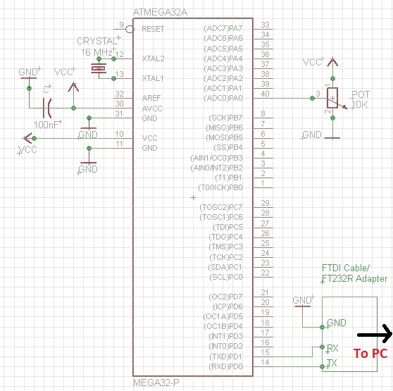
Let’s start by doing a simple test program so we can see our ADC in action. For this our atmega will read an 10Kohm POT connected to pin 0 of PORT A, that is the PA0 pin of ATmega32A, and the read value of POT will be displayed on serial terminal of PC. We’ll use USART Code Libraries for serial communication.
CONNECTIONS: ADC in AVR ATmega32A Microcontroller
The pot will be connected as shown in following schematic:
To make use the ADC in AVR ATmega32A Microcontroller. We have to perform some steps. Here is pseudo-code and this is what we need to do:
- Configure ADC
- Turn ON ADC
- Start ADC Conversion
- Read ADC value from ADC Data Register
Here is complete C Program to use ADC in AVR ATmega32A Microcontroller. Later on in this tutorial we’ll slice down program into several pieces to get more inside view.
#define F_CPU 16000000UL

#include <avr/io.h>
#include <stdlib.h>
#include <util/delay.h>

#define BAUDRATE 9600
#define BAUD_PRESCALLER (((F_CPU / (BAUDRATE * 16UL))) - 1)

uint16_t adc_value;			//Variable used to store the value read from the ADC
char buffer[5];				//Output of the itoa function

void adc_init(void);			//Function to initialize/configure the ADC
uint16_t read_adc(uint8_t channel);	//Function to read an arbitrary analog channel/pin
void USART_init(void);			//Function to initialize and configure the USART/serial
void USART_send( unsigned char data);   //Function that sends a char over the serial port
void USART_putstring(char* StringPtr);   //Function that sends a string over the serial port

int main(void){
  adc_init();							//Setup the ADC
  USART_init();						//Setup the USART

  while(1)							//Our infinite loop
  {
    USART_putstring("Reading channel 0: ");
    adc_value = read_adc(0);
    itoa(adc_value, buffer, 10);
    USART_putstring(buffer);
    USART_putstring("  ");
    _delay_ms(500);
    USART_send('\r');
    USART_send('\n');                //This two lines are to tell to the terminal to change line
  }
  return 0;
}

void adc_init(void){
  ADCSRA |= ((1<<ADPS2)|(1<<ADPS1)|(1<<ADPS0));   // 16Mhz/128 = 125Khz the ADC reference clock
  ADMUX |= (1<<REFS0);							// Voltage reference from Avcc (5v)
  ADCSRA |= (1<<ADEN);							// Turn on ADC
  ADCSRA |= (1<<ADSC);							// Do an initial conversion because this one is the slowest and to ensure that everything is up and running
}

uint16_t read_adc(uint8_t channel){
  ADMUX &= 0xF0;							// Clear the older channel that was read
  ADMUX |= channel;							// Defines the new ADC channel to be read
  ADCSRA |= (1<<ADSC);							// Starts a new conversion
  while(ADCSRA & (1<<ADSC));						// Wait until the conversion is done
  return ADCW;								// Returns the ADC value of the chosen channel
}

void USART_init(void){
  UBRRH = (uint8_t)(BAUD_PRESCALLER>>8);
  UBRRL = (uint8_t)(BAUD_PRESCALLER);
  UCSRB = (1<<RXEN)|(1<<TXEN);
  UCSRC = (1<<UCSZ0)|(1<<UCSZ1)|(1<<URSEL);
}

void USART_send( unsigned char data){
  while(!(UCSRA & (1<<UDRE)));
  UDR = data;
}

void USART_putstring(char* StringPtr){
  while(*StringPtr != 0x00){
    USART_send(*StringPtr);
  StringPtr++;}
}
CODE EXPLANATION:
First few lines represent some standard includes that we’ll be using while structuring our code. If you compare code from previous tutorial you’ll find lots of similarities. Here we’ll only discuss functions which are added into previous project. I recommend you to grab a datasheet and jump right on Chapter:22 and Page No: 223. Apart from that in main function.
void adc_init(void){
  ADCSRA |= ((1<<ADPS2)|(1<<ADPS1)|(1<<ADPS0));   // 16Mhz/128 = 125Khz the ADC reference clock
  ADMUX |= (1<<REFS0);				// Voltage reference from Avcc (5v)
  ADCSRA |= (1<<ADEN);				// Turn on ADC
  ADCSRA |= (1<<ADSC);				// Do an initial conversion because this one is the slowest and to ensure that everything is up and running
}
First we need to provide a clock to the ADC, and as we have seen before this signal as a maximum recommended value and this clock is generated using prescaler, so let’s first setup our prescaler. This is configured in the ADCSRA register and the bits that are related to the prescaler settings are ADPS2, ADPS1 and ADPS0, you can see on page no: 226 the possible values for the prescaler are 2, 4, 8, 16, 32, 64 and 128, as we are running at 16Mhz we will use the 128 prescaler so our ADC clock will be of 125Khz (16000000/128= 125 Khz), to set this value we need to set the three ADPS bits to 1.
Now we will configure the voltage reference that our ADC will use, in this tutorial we will use the voltage that is also used to power the rest of our ATmega (+5v), with a external capacitor connected to AVCC pin. The reference voltage source is configured in the ADMUX register with the REFS0 and REFS1 bits. In our case we will make REFS0 bit to 1, it’s also in the ADMUX register that we can select which channel will be used to perform an analog to digital conversion, this is selected using the MUX3 to MUX0 bits, in this example we’ll not touch this bits as we are reading from channel 0 and all the bits in the registers are in the 0 state when we power up our ATmega.
Now our ADC is almost setup, we just need to turn it on (because by default it’s turned off so the micro-controller consumes less current), and for that we put the ADEN bit at 1 in the ADCSRA register. Remaining things are well commented into code itself.
uint16_t read_adc(uint8_t channel){
  ADMUX &= 0xF0;							// Clear the older channel that was read
  ADMUX |= channel;							// Defines the new ADC channel to be read
  ADCSRA |= (1<<ADSC);							// Starts a new conversion
  while(ADCSRA & (1<<ADSC));						// Wait until the conversion is done
  return ADCW;								// Returns the ADC value of the chosen channel
}
Now here in this function we have to select the ADC input channel. In this example we’re going to read data from channel 0 which is PA0 pin of ATmega chip. It can be done by setting or clearing the MUX4, MUX3, MUX2, MUX1 and MUX0 bits in the ADMUX register, the mapping between the MUX values and the selected channel is shown in this table:
| MUX4 | MUX3 | MUX2 | MUX1 | MUX0 | Pin that will be read |
| 0 | 0 | 0 | 0 | 0 | PORTA0 Analog 0 |
| 0 | 0 | 0 | 0 | 1 | PORTA1 Analog 1 |
| 0 | 0 | 0 | 1 | 1 | PORTA2 Analog 2 |
| 0 | 0 | 0 | 0 | 0 | PORTA3 Analog3 |
| 0 | 0 | 1 | 0 | 0 | PORTA4 Analog 4 |
| 0 | 0 | 1 | 0 | 1 | PORTA5 Analog 5 |
| 0 | 0 | 1 | 1 | 0 | PORTA6 Analog 6 |
| 0 | 0 | 1 | 1 | 1 | PORTA7 Analog 7 |
when running in single conversion mode there are some new things that we must check, as the ADC clock is rather slow (125Khz compared to the 16Mhz that the chip is running) and each conversion takes 13 cycles of that 125Khz clock when we read the ADC we start a new single conversion and we need to wait until it’s done, to do this we check the bit ADSC until its cleared, when its cleared the conversion is done, and as we are doing single conversions we don’t need to mess with the ADTS and ADATE bits.
The code is still easy to read and understand, and now we have two handy functions that you can just copy and paste into your projects and read the ADC, the number that you pass to the read_adc(). It’s also the pin number from PORTA, so analog channel 0 is in PORTA0 and can be read using read_adc(0). The remaining setting is well commented in code itself and self explanatory.
You may wonder what is ADCW? Where does it come from? Its AVR LIBC function which supported by most of avr-gcc compilers, where we get result of ADC conversion. This could be handy instead of shifting bits to get 10 bit result from ADCH and ADCL. These are ADC Data Registers.
while(1)					 //Our infinite loop
  {
    USART_putstring("Reading channel 0: ");
    adc_value = read_adc(0);
    itoa(adc_value, buffer, 10);
    USART_putstring(buffer);
    USART_putstring("  ");
    _delay_ms(500);
    USART_send('\r');
    USART_send('\n');                //This two lines are to tell to the terminal to change line
  }
In never ending loop We’ll read the ADC converted value, and this has done using simple function read_adc(0). In order to convert the 10 bits ADC value to a readable number string we need to use a function called ITOA(stands for Integer TO ASCII) this function takes 3 input parameters, one is the value that we want to convert, this can be an uint8_t, uint16_t, int, and other similar types of integer variables, other of the input parameters is the base for where we want to convert, 2 to convert to binary, 8 for octal, 10 for decimal, and 16 for hexadecimal, and finally a small array that will be the output string plus the NULL string terminator, this output array must have at least space for the maximum number of chars that our number as plus one for the NULL, so as we are using 10 bits values from the ADC, this means that our maximum value is 2^10-1 = 1023, so we can have a maximum of 4 numbers plus the terminator so we need an array with space for 5 chars. Also, itoa is one of the standard functions of C, and thus it is located in the stdlib.h header and that header must be included so the compiler doesn’t complain.
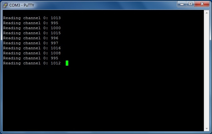
When we compile and download output file to AVR ATmega32A (Make sure to set fuse bits). We’ll get ADC output on serial terminal of PC. Here is output from our project.
We hope you will find this tutorial educational and entertaining to use ADC in AVR ATmega32A Microcontroller. If you have any question then post into comment section of website.