This tutorial covers transistor basics and conceptually answer a question how transistor works? A good understanding of transistor is essential for working on electronic circuits. Transistors are backbone of electronics. They are everywhere; in discrete form, in group of millions as integrated circuit. We will explore each and every aspect of transistor in this section of tutorial series.
Table of Contents
Concepts You Must Know
Before going on journey of transistors, we recommend you to have a look on some basics linked with transistors. The construction and working of transistor is related to diodes, you are suggested to read tutorials on diodes and basic electronics.
You will see the concept of conventional current v/s electron flow in this tutorial couple of times. As the name suggest conventional current is traditional, old fashion way of expressing the concept of current. Conventional current flows from Positive to Negative. Yes, that looks conceptually wrong but, you may find its proof in diode symbol. Electron with its negative charge get easily attracted towards positive source. Hence electron flow is from Negative to Positive. These concepts seem confusing, but they are very clear and both are acceptable. It doesn’t matter which direction of current flow is considered, what matters is using the same direction consistently. The job of current in electronic circuit doesn’t change with direction of current flow.
Why We Use Transistor?
Today, most of the electronic circuits are consists of integrated circuits (ICs). There are millions of transistors hidden in an integrated circuit like Microcontroller. The input-output configuration of such ICs is based on transistors. Transistors have many advantages like small size, easy availability, low cost, easy to use. They are responsible for shrinking electronic circuits. You might be thinking that what does a transistor actually do? So, besides amplification (turning low power signal to similar high power signal) transistors can also act as switch. With this combo abilities transistors can do a lot. With its switching and signal amplifying ability transistor replaced use of mechanical switch and vacuum tube in electronics. Like other electronic components we have discussed so far, transistors do have various types for variety of applications. That’s why transistor is vital part of electronics.
What is Transistor?
Electronics is about using extremely minute particles called electrons; to control electricity. Transistor controls electricity with electrons. The first transistor is practically implemented in 1947 by physicists John Bardeen, Walter Brattain, and William Shockley. This transistor was named as point-contact transistor. Later on William Shockley invented bipolar transistors in 1948. A transistor is simple active electronic device by its physical structure and little bit complex by its working. By definition, a transistor is a two pn junction semiconductor device used as a switch or to amplify electronic signals.
The prefix trans tells about signal transfer from low resistance to high resistance part and istor means solid physical structure having property of resistance.
Bi-polar Junction Transistor (BJT)
The transistors are divided into two main types: bi-polar junction transistors (BJT) and field effect transistors (FET). In transistor tutorials we will learn each and every variation of both types in detail. The most common transistor we use is junction transistor (BJT). Hence most of people working with electronics use the word transistor for referring BJT. You might be thinking about the name bi-polar, why so called? We will see the reason behind this in transistor working. Now, from here we will learn about BJTs, its types, construction, working etc.’
Transistor Symbols
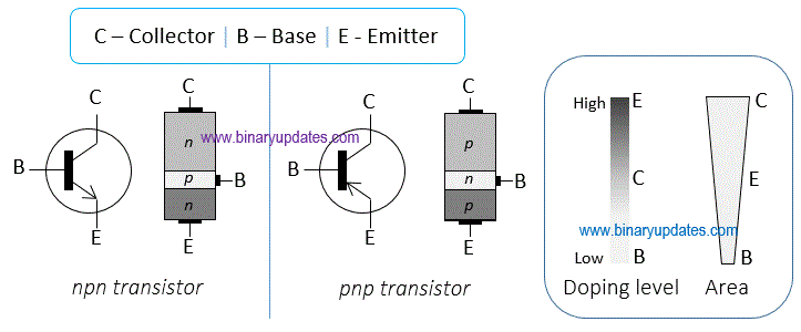
Transistors are conceptually 3 terminal active devices. These 3 terminals are named as collector (C), base (B) and emitter (E). A transistor has a 3 sandwich layers of doped semiconductors. The layer combination can be either npn or pnp.
1) npn = Not Pointing iN, pnp = Pointing iN
2) Using concept of conventional current arrow direction for npn is np->n and for pnp is p->np
Transistor Construction
In construction of BJT, middle region is named as base and outer 2 regions are emitter and collector. In figure above, you may find outer layers similar, but their operations are much different in terms of electrical and physical properties. The doping level of emitter is highest and base is lowest. The collector region has largest area and base has smallest area. You might be wondering about largest size of collector region. The reason is during practical working of transistor, heat (wasted power) is generated at collector. As compare to other regions the collector area in transistor is made larger to dissipate heat.
The construction of transistor is actually extension of pn junction structure of diode. Hence a transistor can be visualize as two diodes with their anodes (NPN) or cathodes (PNP) link together. The pointing direction of arrow in BJT symbol can be verified from position of diode. In case of NPN diode is pointing towards emitter and for PNP, diode is pointing towards base. This pointing direction tells about direction of current flow through the transistor.

Transistor in Action
A transistor working can be demonstrated by extending water analogies of resistor and capacitor. In water analogy of transistor, we consider width of the pipe as resistance, current is water flow and pressure pushing that water through a pipe is voltage. The transistor is analogues to a valve. The handle of this valve is transistor base pin which allow more or less electrons to flow from emitter to collector. The operation of transistor as a switch (ON / OFF) and amplifier can be explain with water valve by controlling the water flow rate.
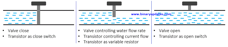
Similar to valve controlling water flow rate, transistor can also control current flow by slight tuning of base current. Hence bipolar transistor is called as current controlled device. The amplifying characteristics of transistors make them special electronic device.
Transistor Working
There are two similar doped semiconductor outer regions in both npn and pnp transistor i.e. emitter and collector. As the name suggest emitter emits charge carriers to base. The collector collects charge carriers from base to pass them along to the next part of circuit. The base controls charge carriers flowing through layers. The base is like door or gate controlling current in transistor.
The term “charge carriers” is used to indicate electrons (-ve charge) and holes (+ve charge) in case of npn and pnp respectively. Conceptually, holes are nothing but absence of electrons.
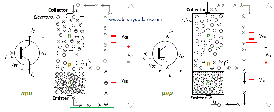
The emitter is forward bias with respect to base to emit or supply large number of charge carriers. The collector is reverse bias w.r.t. base to collect charge carriers emitted by emitter. The forward or reverse biasing of respective transistor region depends on application where transistor will to be used. The emitter is heavily doped, hence need very small amount of pressure (voltage) is required to push charge carriers from emitter to base. According to diode analogy of transistor, an emitter-base part if equivalent to diode. The forward voltage of diode is around 0.6 V. Hence a small amount of voltage is required to forward bias emitter w.r.t. base. The collector is lightly doped than emitter hence more voltage is applied at collector than emitter.
In electronics, bias is a constant DC voltage or current. In biasing a constant DC voltage is purposely applied between two terminals in order to control electronic device. E.g. Biasing voltage of around 0.6 V will turn ON transistor.
Working of npn Transistor
The forward bias emitter emits electrons to base. These electrons constitutes emitter current (IE). Very few electrons from emitter combines with holes at base which make base current (IB). The remaining electrons easily pass lightly doped base region and make collector current (IC). So, we can say that approximately complete emitter current flows in collector part. In npn, emitter and base is of n-type and p-type respectively. Hence electrons are the majority carriers and holes are minority carriers.
Working of pnp Transistor
The pnp transistor works very similar to npn transistor. In case of pnp the only difference is due to p-type emitter and n-type base, holes are the majority carriers and electrons are minority carriers. Hence emitter emits holes current conduction in pnp is by holes but, in external conducting path like wires current is by electrons. In pnp transistor negative base voltage controls emitter-collector current flow.
With this discussion we can mathematically define emitter current with Kirchhoff’s current law as,
Since IB is very small; and measure in µA,
IE ≈ IC
That’s enough for this first post on How Transistor Works. There’s a lot more to discuss about transistors. This is just a beginning. I hope now you are familiar with the word transistor. Please check out our next post for a more detailed explanation of the working of a transistor.