This tutorial is about Introduction to ARM7 LPC2148 Microcontroller. We’ll also discuss some facts and features of NXP LPC2148 microcontroller. This guide will help you to understand functional fundamental of ARM7 LPC2148 Microcontroller. In next tutorial, we’ll install software and configure hardware to burn or download hex file into flash memory of LPC2148 Microcontroller.
What is ARM?
ARM-Advanced RISC Machine is a 32-bit RISC (Reduced Instruction Set Computer) processor architecture developed by ARM Holdings. Many beginners sometimes misunderstood that the ARM is microcontroller or processor but in reality, ARM is an architecture which is used in many processors and microcontrollers. The ARM architecture licensed to companies that want to manufacture ARM-based CPUs or System-on-Chip products. This enables the companies to develop their own processors compliant with the ARM instruction set architecture. For example, the device we are using LPC2148 is ARM architecture based SOC product developed by NXP Semiconductor. Similarly, all major semiconductor manufacturers like Atmel, Samsung, TI etc. they all make ARM based SOCs.

Why start with ARM7 LCP2148?
ARM7 is most successful and widely used processor family in embedded system applications. So we have decided to choose ARM7 TDMI based NXP controller LPC2148. Also, ARM7 is a balance between classic and new Cortex series. ARM7 is excellent to get start with in terms of resources available on internet and quality documentation provided by NXP. It suits perfectly for beginners to get in-depth idea about hardware and software implementation.
LPC2148 is manufactured by NXP Semiconductor (Phillips) and it is preloaded with many in-built features and peripherals. This makes it more efficient and reliable choice for an high-end application developer. I don’t want to repeat list of features from User Manual. I request you to hold user manual while reading these tutorials. As we move along, We’ll discuss and use almost all features throughout this series. Now let’s have a look at pin diagram of LPC2148.
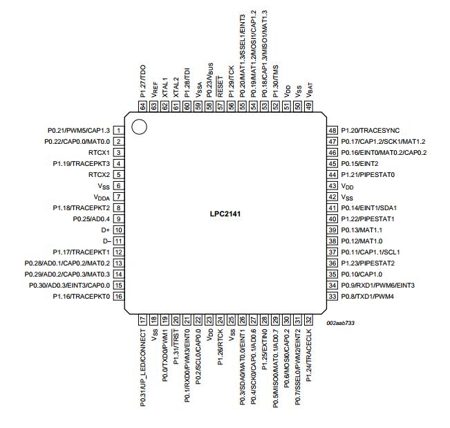
For newbie’s it’s more important to have basic knowledge of pin configuration, memory, IO ports and basic registers.
MEMORY
LPC2148 has 32kB on chip SRAM and 512kB on chip FLASH memory. This chip has built in support up to 2kB end point USB RAM. This memory is more than enough for almost all applications. Let’s understand the function of this huge memory space in LPC2148.
FLASH Memory System: The LPC2148 has 512kB flash memory. This memory may used for both code and data storage. The flash memory can be programmed by various ways
- Using serial built in JTAG Interface
- Using In-System Programming (ISP)
- By means of In-Application Programming (IAP) capabilities
The application program, using IAP functions may also erase and/or program the FLASH while the application is running. When the LPC2148 on chip bootloader is used, 500kB of flash memory is available for user code.
RAM Memory System: LPC2148 provides 32kB of static RAM which may be used for code and/or data storage. It may be accessed as 8-bit, 16-bit and 32-bits.
INPUT/OUTPUT PORTS (GPIO of LPC2148)
Understanding what is IO Ports and how to use them is very important. It’s because when we see micro chip, we’ll find a black box i.e. IC with some pins. LPC2148 has two IO ports each of 32-bit wide, provided by 64 IO pins. Ports are named as P0 and P1. Pins of each port labeled as Px.y where “x” stands for port number, 0 or 1. Where “y” stands for pin number usually between 0 to 31. Each pin can perform multiple functions. For example: Pin no.1 which is P0.21 serves as GPIO as well as PWM5, AD1.6 (A/D converter1, input 6), CAP1.3 (Capture input for Timer1, Channel 3).
CONFIGURE GPIO in LPC2148:
The first thing to learn while programming LPC2148 is how to configure GPIO Pins? Let’s start with the associated concepts and registers.
| PORT PINS | TYPE | DESCRIPTION |
| P0.0-P0.31 P1.16-P1.31 |
Input/output | General purpose input/output. The number of GPIOs actually available depends on the use of alternate functions. |
PORT 0 is a 32-bit I/O port with individual direction controls for each bit. Total of 28 pins of the Port 0 can be used as a general purpose bi-directional digital I/Os while P0.31 provides digital output functions only. The operation of port 0 pins depends upon the pin function selected via the pin connect block. Pins P0.24, P0.26 and P0.27 are not available.
PORT 1 is a 32-bit bi-directional I/O port with individual direction controls for each bit. The operation of port 1 pins depends upon the pin function selected via the pin connect block. Pins 0 through 15 of port 1 are not available.
PORT0 and PORT1 are controlled via two groups of registers explained below.
IOPIN
This is GPIO Port Pin value register. The Current State of the GPIO configured port pins can always be read from this register, regardless of pin direction.
IODIR
This is GPIO Port Direction control register. This register individually Controls the direction of each Port Pin.
IOCLR
This is GPIO Port Output Clear registers. This register controls the state of output pins. Writing ones produces lows at the corresponding port pins and clears the corresponding bits in the IOSET register. Writing zeroes has no effect.
IOSET
This is GPIO Port Output Set registers. This register controls the state of output pins in conjunction with the IOCLR register. Writing ones produces highs at the corresponding port pins. Writing zeroes has no effect.
These are the set of register used to configure I/O Pins. Now let’s move to individual registers in deep.
REGISTERS FOR C PROGRAMMING
IOSEL0
Port 0 has 32 pins (P0.0 to P0.31). Each pin can have multiple functions. On RESET, all pins are configured as GPIO pins. However we can re-configure using the registers IOSEL0 and IOSEL1.
IOSEL0 is used to select function of P0.0 to P0.15. Each pin has up to 4 functions so 2 bits/pin in IOSEL0 is provided for selecting function.
| 00 | Function 0 (Default Function= GPIO) |
| 01 | Function 1 |
| 10 | Function 2 |
| 11 | Function 3 |
IOSEL1
IOSEL1 is used to select function of Pins P0.16 to P0.31
IOSEL2
IOSEL2 is used to select function of Pins P1.16 to P1.31
IO0DIR
IO0DIR is used to configure pins of Port 0-P0 as input or output pins.
1= Output Pin
0= Input Pin
Example: IO0DIR=0x0000FFFF means P0.0 to P0.15 are configured as output pins and P0.16 to P0.31 are configured as input pins.
IO1DIR
IO1DIR is used to configure pins of Port 1-P1 as input or output pins.
1= Output Pin
0= Input Pin
Example: IO1DIR=0xAAAAAAAA means even pins (P1.0, P1.2, P1.4 etc.) are configured as input pins and odd pins (P1.1, P1.3, P1.5 etc.) are configured as input pins.
IO0SET
It is used to set pins of Port0-P0 to logic 1.
Example: IO0SET=0x0000FFFF will set pins P0.0 to P0.15 at logic 1. It will not affect other pins.
IO0CLR
It is used to set pins of Port0-P0 to logic 0.
Example: IO0CLR=0x0000FFFF will set pins P0.0 to P0.15 at logic 0. It will not affect other pins.
IO1SET
It is used to set pins of Port1-P1 to logic 1.
Example: IO1SET=0x0000FFFF will set pins P1.0 to P1.15 at logic 1. It will not affect other pins.
IO1CLR
It is used to set pins of Port1-P1 to logic 0.
Example: IO1CLR=0x0000FFFF will set pins P1.0 to P1.15 at logic 0. It will not affect other pins.
Once the use of above all registers is perfectly understood, you are good to go with programming.
Example: Blink LEDs connected on pins P0.10-P0.13
Step-1: Select the GPIO PORT Pins using PINSEL0.
Step-2: Specify the direction of pins as output using IO0DIR.
Step-3: Set pins P0.10-P0.13 using IO0SET.
Step-4: Clear pins P0.10-P0.13 using IO0CLR.
Step-5: Go to step-2.
Now, using these steps given here, try to write basic program on your own and once it is done, compare with the basic program given here. You can write this program using various techniques. We have given the most basic option for you. In next tutorial, we’ll do software installation and hardware connections to learn how to program LPC2148 Microcontroller. Feel free to leave comment….!!!!